Zynq-7000 AP SoC Boot - Locking and Executing out of L2 Cache Tech Tip
Zynq-7000 AP SoC Boot - Locking and Executing out of L2 Cache Tech Tip
Document History
| Date |
Version |
Author |
Description of Revisions |
| 06/20/13 |
0.1 |
Yashu Gosain |
Initial revision |
| 12/04/14 |
0.2 |
Ravinder Are |
Updated the tech-tip to cover below requirements 1. Integrating PL logic (for AXI Timer) using Vivado Tools 2014.3 versions and creates the bit stream file for flashing. 2. Execute all execution FSBL and App from OCM memory region. 3. Simple Interrupt working design application to demonstrate AXI Timer use in PS application. 4. Added second application: C++ application execution in L2 cache lock mode. |
| 10/26/16 |
0.3 |
Rutuja chavan |
Updated the tech-tip to the tool version 2016.3 |
Summary
In real time embedded systems, sometimes it is required to get predictable behavior from certain piece of code. For example, interrupt service routine with hard real time constraint.To achieve this, L2-cache controller PL-310 integrated in ZYNQ-7000 SoC provides a feature to lock piece of critical code or data in the cache. Locking of data or code in cache is an indication to cache replacement algorithm to prevent these entries from being evicted. This project is intended to show how to lock critical code or data in L2 cache so that it will not get evicted by replacement algorithm. It provides details about how to preload load data/code into the L2-cache and lock it.
L1 Instruction and Data caches are disabled in this flow, this is done because the code to lock in L2-cache is small code and if L1 cache is enabled and whole application code probably fit inside it and gets executed from there only.
This tech-tip helps user to understand about how to preload data/code in to L2-cache and also how to do use L2-cache Lockdown feature. It also provides a sample application, which user can use in their application code for locking critical code/data in the L2-cache, illustrates the PL AXI Timer working in PS with interrupt triggering and servicing it in an application. It has a second application to demonstrate the C++ based applications development in L2 cache locking mode
Following points are covered in this tip.
- Provide sample routine to do preloading of the code/data segment to L2-cache, in FSBL.
- Shows L2-cache Lockdown feature in Zynq-7000 SOC.
- Reference design for AXI Timer in PL, PL-to-PS working concept demoed.
- Bit Stream file added while generating BOOT.bin file for flashing the Zynq device.
- Shows Interrupt working concept.
- C++ application to run in L2-cache lock down mode.
Implementation
| Implementation Details |
|
| Design Type |
PS + PL |
| SW Type |
Standalone (SMP) |
| CPUs |
2 ARM Cortex-A9 667MHZ |
| PS Features |
|
| PS Features |
BRAM with ECC enabled |
| Boards/Tools |
ZC702 |
| Xilinx Tools Version |
VIVADO version 2016.3. SDK 2016.3 (comes with Vivado installation) |
| Files Provided |
|
| Zynq7000AP_SoC_LockExecuteOutOfL2Cache.zip |
See Appendix A for the descriptions of the files |
1. Description
Whole project demonstrating the above discussed features are part of multiple sections of the design,which have PS section, PL section, and Application sections.
1.1 PS (Processing System section)
Zynq-7000 SoC PS has an inbuilt PL310 Cache controller to manage L2 cache. It is used to improve the performance of ARM based systems when significant memory traffic is generated by the processor. The cache controller provides a cache lockdown feature which can help to lock a critical piece of code or data in to L2-cache. This feature is useful where there is a need to provide deterministic response. Cache controller supports following two lock-down schemes:
- Line based Locking
- Way- based locking
L2-cache and lock it. Details of the modifications are provided in the subsequent sections.
Note: For more detail about the PL310 cache controller, refer to ug585-Zynq-7000-TRM “Zynq-7000 SoC Technical Reference Manual”.
Zynq-7000 SoC PS has an inbuilt PL390 Interrupt controller for configuring and using it for all internal and external interrupt sources for servicing them.
Note: For more details about Generic Interrupt controller, refer to http://infocenter.arm.com/help/topic/com.arm.doc.ddi0416b/
Reference design is based on Zynq 7000 series. All the reference platform selections are Zynq-7ZC702Evaluation Board
1.2 PL (Programmable Logic Section)
This Tech-tip reference design has AXI-Timer IP integrated in PL and provides steps to generate an output ‘bit-stream’ file for flashing the Zynq board along with the other Boot files. The AXI Timer/Counter is a 32/64-bit timer module that attaches to the AXI4-lite interface, It is a general purpose timer/counter with user configurable options.
Note: For more detail about the AXI Timer IP, refer to http://www.xilinx.com/support/documentation/ip_documentation/axi_timer/v2_0/pg079-axi-timer.pdf
User can use Xilinx Vivado® Design Suite to integrate AXI Timer IP with zc702 PS platform. Connect the AXI Timer with Global Interrupt controller (i.e. GIC) in PS. Follow the regular Vivado project steps through bit stream file generation.Next coming sections have detailed information on creating a new Vivado project, integrating the AXI Timer. Also has information on using the reference HW project.
Note: for more details on using Vivado tools, refer to Vivado Design Suite User Guide: Getting Started (UG910) http://www.xilinx.com/support/documentation/sw_manuals/xilinx2014_3/ug910-vivado-getting-started.pdf
1.3 Memory Map, Boot flow and Reference Applications
This tech-tip describes the Boot flow of Zynq -7000 series platforms and provide details on application pre-loading in to L2 cache, locking it, and executing application out of L2 cache. It covers both C, and Cpp based application for demonstration.
OCM Memory Map:
Zynq-7000 series platform has On-chip memory of 256KB, default address range at 0000_0000 to 0003_FFFF of 192kB and FFFC_0000 to FFFF_FFFF of 64KB.
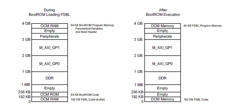 |
| Figure 1: System Memory Map during and after Boot-ROM Execution |
Boot flow:
The Zynq platform’s default boot loader functionality is split into two different small programs. Boot-ROM code and the First Stage boot loader (FSBL).Boot-ROM executes at start up, loads the FSBL from non-volatile storage to dynamic On Chip Memory (OCM) and executes it. The FSBL can execute from Flash itself, for this boot loader creation (Bootgen tool) need to set the xip_mode attribute. FSBL executes and copies the application from non-volatile memory to external DDR memory, and transfer control to application start address to execute it.
This tech-tip has some modifications in boot loader and its sequence to accomplish the “application preloading to L2 cache, locking L2 cache and executing it”. Zynq Boot code is spread in FSBL and FSBL_bsp projects. Refer to the software_projects.zip for the reference design files.
Boot flow changes in this tech-tip:
1. In this tech-tip, FSBL executes from OCM memory
2. FSBL checks for application segments that need to be preloaded (preload_funct() function) in to L2 and loads them. PartitionMove() function has changes.
3. Afterapplication loading the Boot flow is same as regular one discussed above.
FSBL Software flow for preloading application to L2 cache and locking it:
- Set page table entry attribute to “No Inner cacheable and No Outer cacheable” for OCM memory region used for FSBL. In the reference example FSBL runs from OCM memory, range 0x00000000 - 0x30000000
- Set page table entry attribute to “Inner and outer cacheable” , for FLASH linear memory region used for Application code segments loading address. In the reference example Applications use linear FLASH memory, range 0xfc700000 - 0xfdffffff set to Outer
- Cacheable but not Inner cacheable.
- Invalidate Instruction cache.
- Invalidate both L1 and L2 data caches.
- Disable both L1 instruction as well as data caches.
- Preload and Lock the data in the L2-cache
- Locked all the 8 ways of L2-cache
Changes to the default FSBL and FSBL_bsp files:
- translation_table.s file in FSBL_bsp has modified to have the MMU translation table entries changes.
- lscript.ld file changed to accommodate the linker changes in FSBL.
- main.c in FSBL changed to have the “preload_func “ function.
- In fsblhandoff.s file, FsblHandOffExit function is modified by commenting out disabling of MMU and invalidating cache assembly code while handing off to application.
- In image_mover.c the PartitionMove() function has modified by commenting some code.
- In qspi.c the initQspi() and qspi access functions modified ,changes present provided reference design projects the design files of this tech tip. These modifications’ eliminates the re-initialization of the qspi.
- Code changes with ‘’DDRLESS_SYSTEM” macro protection in multiple FSBL files.
FSBL Linker script:
FSBL linker script use the below memory ranges
MEMORY
{
 ps7_ram_0_S_AXI_BASEADDR : ORIGIN = 0x00000000, LENGTH = 0x00030000
 ps7_ram_0_S_AXI_BASEADDR_sub : ORIGIN = 0x0002FF00, LENGTH = 0x000100
 ps7_ram_1_S_AXI_BASEADDR : ORIGIN = 0xFFFF0000, LENGTH = 0x0000F800
}
ps7_ram_0_S_AXI_BASEADDR_sub : OCM memory used for “Interrupt vector table” it is initialized in FSBL and will be continued to be used in Application without any modification, Applications also have reserved same region for vector table.
ps7_ram_1_S_AXI_BASEADDR: OCM memory used for FSBL stacks and heap sections.
Importing and building FSBL application is described and discussed in next sections.
C Application:
This is a simple C application, which makes use of AXI Timer integrated in PL.
It initializes the interrupt controller, configures the AXI Timer with counter value and call back handler, also registers timer interrupt service routine. For every timer timeout, interrupt triggers and timer Interrupt handler executes (ISR routine).
All the required bsp files for building the application are linked with this application by copying them in to same project source path, they are Timer, interrupt controller, UART (for serial prints).
C-Application software flow:
- Entry point for the application code is set to _startcode which is defined in the startup.s assembly file. At this entry point, stack pointer memory location is assigned to Stack pointer register and then branch to main() function.
- main() function is defined in Application.c file. It performs following operation.
- copy the data section from FLASH(load region) to OCM(Execution region) memory region.
- Copy the Interrupt vector table from FLASH(load region) to OCM(Execution region) memory region.
- configures PL timer.
- Associate timer ISR with the Timer interrupts.
- initialize the Interrupt controller.
- start the timer and wait for timer triggering through interrupt..
- Prints log messages inside ISR routine.
C-Application Linker Script: Application linker script defined following memory sections.
MEMORY
{
 FLASH: ORIGIN = 0xFC700000, LENGTH = 0x200000
 ps7_ram_0_S_AXI_BASEADDR: ORIGIN = 0x00020000, LENGTH =  0x00030000
 ps7_ram_1_S_AXI_BASEADDR: ORIGIN = 0x0002ff00, LENGTH = 0x000100
}
ps7_ram_0_S_AXI_BASEADDR: OCM memory used for application’s “data”, “stack”, “heap” sections.
ps7_ram_1_S_AXI_BASEADDR: OCM memory used for “Interrupt vector table” it is initialized in FSBL and will be continued to be used in Application without any modification, Applications also have reserved same region for vector table.
CPP- Application:
It setups the c++ runtime required infrastructure like global objects construction and destruction. Also it demonstrates the basic mathematics based c++ class defining and using them. It has simple classes defined for mathematical operations such as Summation and Multiplication, and using them.
CPP-Application software flow
- Entry point for the application code is set to _startcode which is defined in the startup.s assembly file. At this entry point, stack pointer memory location is assigned to Stack pointer register.
- Then it branches to copyRO () function which defined in copyRO.cc file to copy the Application own data segments to OCM.
- Then it branches to libc_init_array() function to executes all global constructors which have static objects used across the application.
- Then it branches to main() function in app.cc file , where it defineclasses for Multiplication (class name ‘Mult’) and Summation (class name ‘Sum’) and carryout the math operations using the objects.
- While exiting it calls libc_fini_array() to cleanup all global static objects by calling destructors.
MEMORY
{
 ps7_ram_0_S_AXI_BASEADDR : ORIGIN = 0x00010000, LENGTH = 0x00020000
 FLASH : ORIGIN = 0xFC700000, LENGTH = 0x2FE000
}
FLASH: QSPI flash memory used for applications code and read only data segments load address region.
2. Hardware and Application Software Development using Xilinx Vivado & SDK tools
2.1 Hardware Development
This section describes steps about the hardware generation and exports it to SDK.
Using reference design files:
- Reference design files shared has system_top_wrapper design Vivado project.
- Open Vivado tool and source the project.tcl file shared in reference design in this tech-tip.
- Source project.tcl file, which will launch the project with the reference design showing below. project.tcl is under “HW_design” folder in Reference design files.
- To rebuild and generate the bit stream file, run generate bit-stream in Vivado tool.
- Start Vivado tool 2016.3.
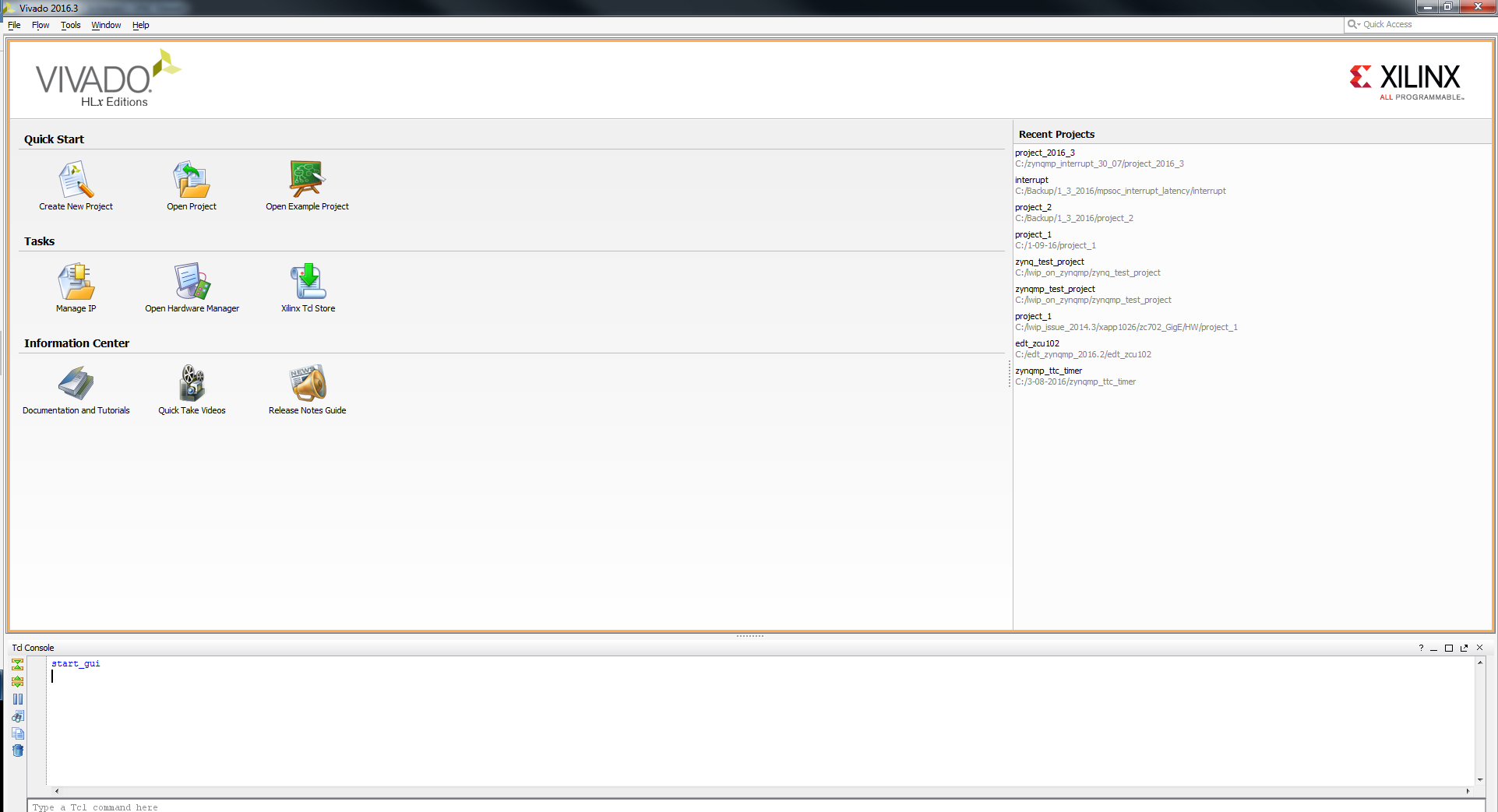 |
| Figure 2: Vivado tool 2016.3 |
2. In “Tcl_Console” command prompt , cd to the HW project files path C:\Reference_Design_Files\HW_design\
source project.tcl , it will create a new HW project with the reference design of AXI in PL.
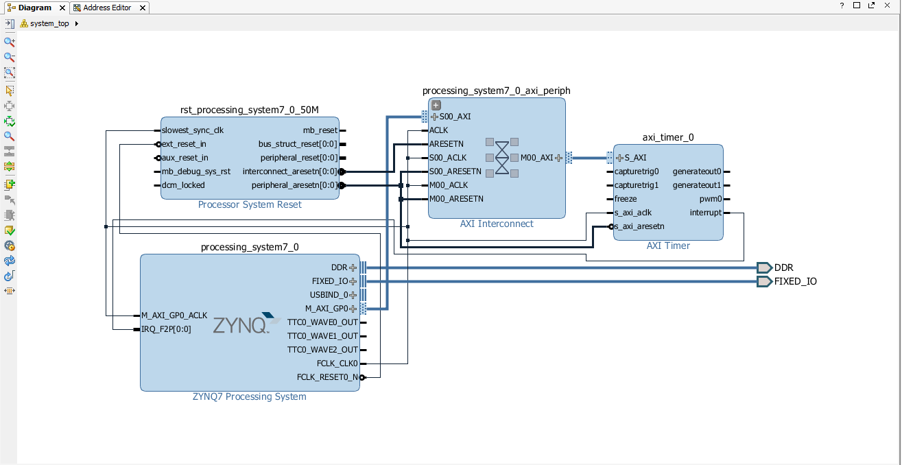 |
| Figure 3: Block diagram |
3.In the Flow Navigator > tab click on the Generate Bit stream
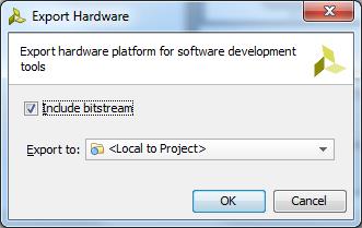
4.Then, Go to the File->Export-> click on Export hardware, The Export hardware diagram opens, then enable the Include bitstream and click ok.
SDK launching and importing the software project files
5. For this go to the File-> click on Launch SDK.
6. The SDK window will be launched.
2.2 Application Software Development
This section describes about the application development and creation of the booting image. This booting image is used for boot the ZYNQ device and running the application from L2 cache. If user wants to skip this section and jump Application Execution, then prebuilt image (BOOT.bin) is included and located in the directory C:\Reference_Design_Files\generated_files\ and it can be used.
After SDK launch, the projects can be imported to use the provided reference design files.
1. Select File->Import to open an import wizard.
2. Select General > Existing Projects into Workspace in the import wizard.
3. Select Achieve file software_projects.zip and specify the location where the software applications are stored.
4. The import wizard displays a list of projects that are available to import. This list Includes
- fsbl_xip
- fsbl_xip_bsp
- Application
- Application_Cpp
- Select all these projects and click Finish
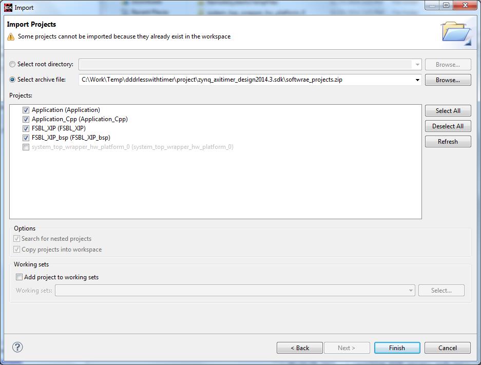 |
| Figure 4: Importing Existing project into SDK workspace |
2.3 Generating Boot File
This tech-tip boot file contains FSBL (fsbl_XIP.elf), PL Bit stream file (system_top_wrapper.bit) and Application (Application.elf/Application_Cpp.elf) binaries.
Followings are the steps to create Boot file
1. In SDK, select Xilinx Tools > Create Boot Image. The Create Zynq Boot Image wizard opens.
2. Provide the FSBL_XIP.elf , Bit stream file and Application elf files. Provide the proper offset for the build file generation against every executable.Please refer the bootimage.bif shared under reference files.
Note :
- find fsbl_XIP. Elf in <SDK Workspace\ fsbl_XIP\Debug\fsbl_XIP.elf
- find .bit file in <SDK >\ system_top_wrapper_hw_platform_0\system_top_wrapper.bit
- find Application. Elf in <SDK Workspace\ Application\Debug\Application.elf
4. Click Create Image.
The Create Zynq Boot Image can be created as one of the following files in the specified output folder
- <filename>.bin
- <filename>.mcs
Using the Reference design projects:
Modify the path of binaries and Import the bootgen file “bootimage.bif” or “bootimage_Cpp.bif” for creating the Boot gen file based on C or Cpp choice.
3 Application Execution:
Follow the below procedure to execute application on the board
1. Make sure that the hardware board is set up is done properly.
Note: RefertoUG873, Zynq-7000 SoC: Concepts, Tools, and Techniques, section2.1.3 TakeTestDrive!Runningthe“HelloWorld” Applicationfor information about setting up the board
2. Change the SW16 switch setting as shown below to set the board to JTag flash mode.
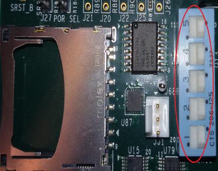 |
| Figure 5: JTAG mode switch settings |
Note: Configuration for Zynq Processing System is: Baud rate 115200; 8 bit; Parity: none; Stop: 1 bit; Flow control: none.
4. Flash the BOOT.bin to Zynq QSPI flash memory.
Note: either use prebuilt BOOT.bin/Boot_Cpp.bin files provided with the reference design files under following directory C:\Reference_Design_Files\generated_files\ Or use BOOT.bin generated in the above section.
5. Change SW16 switch setting as shown below to change the booting type to QSPI booting.
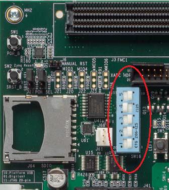 |
| Figure 6: Flash mode switch settings |
6. Power ON the board.
7. Check the serial communication utility for the message.
8. After successful execution, message showing Application execution.
4.Expected Result
C Application:
Trace messages dumped on Serial terminal.
##### Timer demo Starts #####
@@@@@@@@@@@@@@@@@@@@@@@@@@@@@
Inside Timer ISR
Timer ISR Exit
@@@@@@@@@@@@@@@@@@@@@@@@@@@@@
Cpp Application:
Trace messages dumped on Serial terminal.
Addition Starts ...
Sum: 1+1 = 2
Addition Done
#####################################
Multiplication Starts...
#####################################
Multiplication: 1*1 = 1
Multiplication Done
#####################################
5 Appendix A: File Descriptions in the design_file directory
Directory Structure of the shared source files.
- Zynq7000AP_SoC_LockExecuteOutOfL2Cache_update_2016_3.zip
- Reference_Design_files
- Bootgen: It contains boot image format configuration data, C and Cpp applications have separate bootgen files.
- bootimage.bif : Bootgen file for C application.
- bootimage_Cpp.bif : Bootgen file for Cpp application.
- generated_files
- Application.elf: C Application Executable file.
- Application_Cpp.elf:
- BOOT.bin : flash able executable.
- BOOT_Cpp.bin : flash able executable.
- FSBL_XIP.elf: FSBL executable.
- system_top_wrapper.bit : bit stream file generated by Vivado tool.
- HW_design
- project.tcl
- system_top.tcl
- system_top_wrapper.v
- softwrae_projects.zip -contains source code files for
- fsbl,
- fsbl_bsp,
- Application,
- Application_Cpp
- Result
- C_Application_Result.txt: It contains the result data after executing C application.
- Cpp_Application_Result.txt: It contains the result data after executing Cpp application
- Bootgen: It contains boot image format configuration data, C and Cpp applications have separate bootgen files.
© Copyright 2019 - 2022 Xilinx Inc. Privacy Policy