Zynq-7000 AP SoC - Using BRAM for Additional On-Chip Memory Tech Tip
Zynq-7000 AP SoC - Using BRAM for Additional On-Chip Memory Tech Tip
Document History
Table of Contents
| Date |
Version |
Author |
Description of Revisions |
| 04/30/13 |
0.1 |
YASHU GOSAIN |
Initial Revision |
Description/Summary
This project is intended to show the integration of programmable logic (PL) BRAMs with the processing system (PS). It provides details about enabling the ECC feature for BRAMs, also shows how to connect the ECC related interrupt with the Global Interrupt Controller (GIC) in PS and also the steps for the integration. In the latter sections, it also show how to build an basic read and write application to verify the BRAM connected in the system.
Implementation
| Implementation Details |
|
| Design Type |
PS & PL |
| SW Type |
Standalone |
| CPUs |
1 ARM Cortex-A9 667MHZ |
| PS Features |
DDR3 553 MHz Global Interrupt Controller |
| BRAM blocks |
|
| Boards/Tools |
ZC702. |
| Xilinx Tools Version |
EDK 14.5 |
| Address Map |
|||
| Base_Address |
Size |
Interface |
|
| axi_bram_ctrl |
0x78600000 |
64K |
S_AXI |
| Files Provided |
|
| designfile.zip |
See Appendix A for the contents details |
1. PL BRAM with ECC enabled design for ZYNQ FPGA:
This section describes steps to integrate PL BRAM blocks with PS. It also shows how to enable the ECC capabilities on the PL BRAM blocks and also connection of ECC interrupt with PS GIC module. The block diagram for the system is as shown in Figure 1 |
| Figure 1: Block Diagram |
This system covers the following connections:
- Instantiation of the AXI BRAM controller in PL. Integration of BRAM controller Slave AXI interfaces with the PS General Purpose (GP) Master AXI Interface.
- Integration of the BRAM controller with the Dual port BRAM of size equivalent to 256KB.
- ECC interrupt of BRAM controller connection with GIC module.
2. Implementation Details:
This section discusses the implementation of the reference design. Instruction for integrating PL BRAM with Zynq PS is provided in Section 2.1 PL BRAM integration with ZYNQ PS. User can follow this section to create a new system. If user wants to skip this section and use prebuilt system, a PlanAhead project for design is provided along in the design files. For using prebuilt system follow steps provided in Section 2.2 Pre-Built BRAM Design2.1. PL BRAM integration with ZYNQ PS
For system creation, you start the ISE® PlanAhead™ design and analysis tool and create a project with an embedded processor system as the top level.- Start the PlanAhead tool.
- Select Create New Project to open the New Project wizard.
- Use the information in the table below to make your selections in the wizard screens.

Table 1 - When you click Finish, the New Project wizard closes and the project you just created opens in the PlanAhead design tool.
- Click Add Sources in the Project Manager. The Add Sources wizard open.
- Select the Add or Create Embedded Sources option and click Next.
- In the Add or Create Embedded Source window, click Create Sub-Design.
- Type a name for the module and click OK. For this example, use the name system.
- Click Finish. The PlanAhead design tool creates your embedded design source project. It recognizes that you have an embedded processor system and starts XPS
- In the dialog box opens to ask if you want to create a Base System using the BSB , click Yes. The first window of the BSB asks you to elect whether to create an AXI-based or PLB-based system.
- Select AXI system and click OK.
- In the Base System Builder wizard, create a project using the settings described in the following table. If no setting or command is indicated in the table, accept the default values.
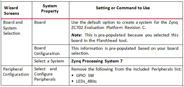
Table 2 - To generate your design,click Finish.
- In the XPS System Assembly View, click the Bus Interfaces tab.
- From the IP catalog, expand Memory and Memory Controller and double-click AXI BRAM Controller to add it. A message appears asking if you want to add the axi_bram_ctrl 1.03.a IP instance to your design.
- Click Yes.
- The configuration window for BRAM Controller opens. Do following in the configuration window
- In the Component instance Name tab, provide to axi_bram_ctrl_0 as an instance name to the IP
- Under System tab, Expand ECC to view the configuration parameters.
- Set Enable ECC functionality.
- Enable Set ECC On/Off Reset Value.
- Click OK. A message window opens with the message "axi_bram_ctrl IP with version number 1.03.a isinstantiated with name axi_bram_ctrl_0." It will ask you to determine to which processor to connect.Remember you are designing with a dual core ARM processor. The message also says XPS will make the Bus Interface Connection, assign the address, and make IO ports external. The default choice of processor is "processing_system7_0". Do not change this.
- Click OK.
- From the IP catalog, expand Memory and Memory Controller and double-click Block RAM (BRAM) Block to add it. A message appears asking if you want to add the bram_block 1.00.a IP instance to your design.
- Click Yes. The configuration window for BRAM opens. Do following in the configuration window
- In the Component instance Name tab, provide to bram_block_0 as an instance name to the IP.
- Click OK.
- Follow the above steps to add AXI Interconnect IP under Bus and Bridge in the IP catalog. Provide axi_interconnect_0 as an instance name to the IP. Use default configuration for AXI Interconnect IP.
- Click the Zynq tab in the XPS System Assembly View to open the Zynq Processing System block diagram.
- Click the green 32b GP AXI Master Port block to open the processing_system7_0 Configuration wizard.
- In the User tab, expand General Purpose Master AXI Interfaces and select the Enable M_AXI_GP0 Interface option
- Click OK to enable the GP Master Port 0 interfaces between the PS and PL.
- Click On the green Clock Generation block to open the clock wizard.
- Expand PL Fabric Clocks.
- Change FCLK_CLK0 Requested Frequency (MHz) to 250.
- Click OK.
- Click the Bus Interfaces tab and make the following connections. Under processing_system7_0, click M_AXI_GP0 and select No Connection in the Bus Name column. Using the drop-down list that appears, connect M_AXI_GP0 to axi_interconnect_0.
- Collapse processing_system7_0.
- Under axi_bram_ctrl_0, click S_AXI, and in the Bus Name column, click No Connection to open the Connection dialog box
- In the Select AXI Interconnect list, click axi_interconnect_0. Notice that processing_system7_0.M_AXI_GP0 appears in the Select Master(s) list. Click the processing_system7_0.M_AXI_GP0 check box to select it.
- Click OK. XPS connects the axi_bram_ctrl_0 Slave port interface with the processing_system7_0 GP master Port 0 interface via axi_interconnect_0
- Follow above steps to connect S_AXI_CTRL port of axi_bram_ctrl_0 with processing_system_0.M_AXI_GP0 via axi_interrconnect_0.
- Collapse axi_bram_ctrl_0.
- Under bram_block_0, click PORTA, and select No Connection in the Bus Name column. Using the drop-down list that appears, connect PORTA to axi_bram_ctrl_0_BRAM_PORTA.
- Under bram_block_0, click PORTB, and select No Connection in the Bus Name column. Using the drop-down list that appears, connect PORTB to axi_bram_ctrl_0_BRAM_PORTB.
- Click the Ports tab, which lists the IPs and their ports. Expand axi_interconnect_0 and axi_bram_ctrl_0.
- Review the following IP connections. If any of these aren't connected, connect them now.

- Collapse all IPs and expand processing_system7_0. If the following port connection is not made, do it now.

- Connect the ECC interrupt on the fabric side to the PS GIC by doing the following
- In the Connected Port column of Processing_System7_0, click L to H: No Connection. The Interrupt Connection dialog box opens.
- In the Unconnected Interrupts list, select axi_bram_ctrl_0 ECC_interrupt and click the right arrow button to move it to the Connected Interrupts list.
- Select axi_bram_ctrl_0 ECC_UE and click the right arrow button to move it to the Connected Interrupts list.
- Click Ok. XPS connects the timer interrupt on the Fabric side to the PS section interrupt controller.
- In the XPS System Assembly View, click the Address tab.
- Click the GenerateAddresses button
 to generate addresses for unmapped devices.
 - In the address map for processing_system7_0, change axi_bram_ctrl_0 IP S_AXI bus interface base address to 0x78600000 and also change the Size field to 256K.
- Change axi_bram_ctrl_0 IP S_AXI_CTRL bus interface base address to 0x78700000.
- Run Design Rule Check. Ensure there are no errors in the console.
- Open system.ucf file from <project_path>\<project_name>.srcs\sources_1\edk\system\data
- Define Clock constraint by adding following two lines in the system.ucf file. NET processing_system7_0/FCLK_CLK0 TNM_NET = clk_fpga_0; TIMESPEC TS_clk_fpga_0 = PERIOD clk_fpga_0 250 MHz HIGH 50%;
- Save system.ucf file.
- Close XPS. The PlanAhead™design tool window becomes active again.
- In Design Sources,click on your embedded sourceand then right-click it and select CreateTop HDL.The PlanAhead tool generates the system_stub.v file.
- Save all modified files.In the Program and Debug list in the Flow Navigator, click Generate Bitstream. Ignore any critical warnings that appear.
- After the Bitstream generation completes,export the hardware and Launch SDK by Selecting File>Export>Export Hardware for SDK. TheExport Hardware dialog box opens.By default,the Export Hardware checkbox is checked.
- Check the Launch SDK checkbox.
- Click OK; SDK opens.
2.2. Pre-Built BRAM Design
The design files should be extracted to a directory called design. After the files have been extracted, a new directory called design\work should be created. Files should be copied as shown:design\src\project to design\work\project
All generated files have been included and are located in the directory
design\generated_files.
2.2.1. Generating Hardware
This section describes the creation of the hardware design. The user can skip this section and go to Section 3Software development and Execution.To implement the embedded design and export it to SDK:
- Start the PlanAhead tool.
- Select Open Project to open embedded project at design\work\project\project_1\project_1.ppr.
- Select Flow > Generate Bitstream to generate bitstream. After it completes, the downloadable FPGA bit file is available at design\work\project\project_1\project_1.runs\impl_1\system_stub.bit.
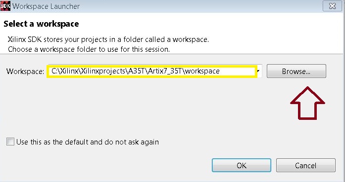
- Export the hardware project to SDK by selecting File > Export > Export Hardware for SDK. Check Launch SDK button to open SDK.
- SDK opens a dialog box asking where the workspace is located. Click OK.
3. Software Development and Execution:
This section describes about the application development and execution on ZC-702 board. For application development and execution user can follow steps mention in Section 3.1 BRAM Application Development and Execution using SDK. If user wants to skip this section, the Prebuilt SD card image (BOOT.bin) is included and located in the directorydesign\generated_files.
User can follow the steps mention in Section 3.2 BRAM application Execution using SD Card to execute prebuilt SD card image on the board.
3.1. BRAM Application Development and Execution using SDK
- In SDK, Select File>New>ApplicationProject. The New Project Wizard opens.
- Use the information in the table below to make your selections in the wizard screens.

- Click Finish. SDK creates the BRAM_app application project and BRAM_app_bsp BSP project under the project explorer.
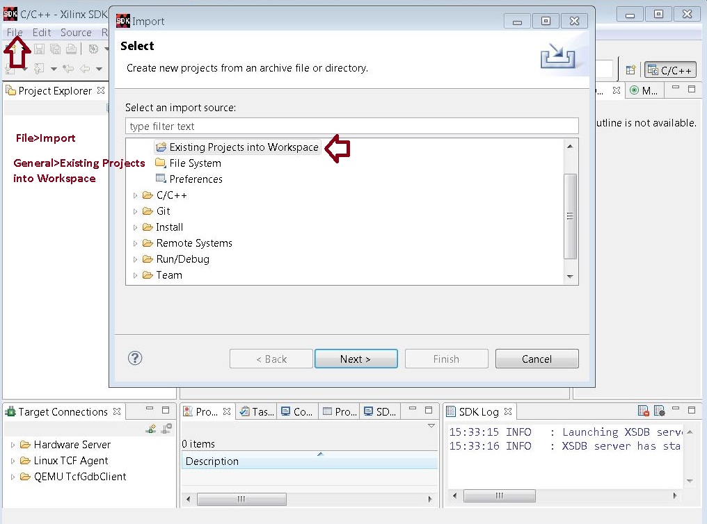
- In the Project Explorer tab,expand the BRAM_app project, right-click the src directory,and select Import to open the new Import dialog box.
- Expand General in the Import dialog box and select File system.
- Click Next
- Add the BRAM_app.c which is located under design\app directory and click Finish. SDK automatically builds the application and displays the status in the console window.
- Make sure that the hardware board is setup and turned on. Note: Refer to UG873, Zynq-7000 SoC: Concepts, Tools, and Techniques, section 2.1.3 TakeTestDrive!Runningthe“HelloWorld” Application for information about setting up the board.
- Open a serial communication utility for the COM port assigned on your system. SDK provides a serial terminal utility;select Window>ShowView>Terminal to open it. Note: The standard configuration for Zynq Processing System is: Baudrate 115200; 8bit; Parity:none;Stop:1bit;Flow control: none.For SDK, you must run the Target Communication Frame (TCF) agent on the host machine. Select Xilinx Tool > Launch Hardware Server.
- In SDK,select Xilinx Tools>Program FPGA to open the Program FPGA dialog box.The dialog box shows the bit stream path.
- Click Program to download the bitstream and program the PL.
- Right-click BRAM_app and select Run as>Run Configurations.
- Right-click Xilinx C/C++ ELF and click New . SDK creates the new run configuration,named BRAM_appDebug. The configurations associated with the application are pre-populated in the Main tab of the launch configurations.
- Click Run.
- Messages get displayed on the serial communication utility.
- After successful verification of the written data to entire BRAM, following message gets displayed. “BRAM Verification successful”
3.2. BRAM Application execution using SD Card
- Make sure that the hardware board is set up is done properly. Note: Refer to UG873, Zynq-7000 SoC: Concepts, Tools, and Techniques, section 2.1.3 Take Test Drive ! Running the“Hello World” Application for information about setting up the board.
- Change the SW16 switch setting as shown below.

- Open a serial communication utility for the COM port. Note: Configuration for Zynq Processing System is: Baud rate 115200; 8bit; Parity: none; Stop: 1 bit; Flow control: none.
- Copy the BOOT.bin under design\generated_files directory to SD Card.
- Insert SD card in the slot provided on the board.
- Power ON the board.
- Check the serial communication utility for the message.
- After successful verification of the written data to entire BRAM, following message gets displayed on serial communication utility. “BRAM Verification successful”
Appendix A: File Descriptions in the Design file diectory
Directory Structure is- Src
- apps
- BRAM_app.c : BRAM software application file.
- project
- project_1 : PlanAhead project directory.
- generated_file
- BOOT.bin: Executable SD card image.
List of Reference:
1. AMBA AXI4 Protocol Specification2. UG761, Xilinx AXI Reference Guide
3. DS777, LogiCORE IP AXI Block RAM (BRAM) Controller (v1.03a)
4. UG873, Zynq-7000 SoC: Concepts, Tools, and Techniques (CTT)
5. UG585, Zynq-7000 SoC: Technical Reference Manual
© Copyright 2019 - 2022 Xilinx Inc. Privacy Policy