Zynq-7000 AP SoC - Performance - Ethernet Packet Inspection - Bare Metal - Redirecting Headers to PL and Cache Tech Tip
Zynq-7000 AP SoC - Performance - Ethernet Packet Inspection - Bare Metal - Redirecting Headers to PL and Cache Tech Tip
Document History
| Date |
Version |
Author |
Description of Revisions |
| 29/06/2013 |
0.1 |
E Srikanth |
Initial Draft |
Table of Contents
1. Introduction
The tech tip provided here is an extension to the “Redirecting Ethernet Packet to PL for Hardware Packet inspection Techtip” provided on the Wiki page. The following tech tip explains how the Ethernet data received by the Gigabit Ethernet Interface on the Zynq PS can be diverted to PL for packet inspection and moved to L2 Cache via the ACP port. The tech tip also benchmarks the amount of time the software needs to process the header while the Ethernet header is directly available in the cache and compared to the header avalible in DDR3 Memory. As will be shown, at the small cost of 10% in packet latency the header read times are cut by 30% for small packets and by 80% for large packets
The design used in this tech tip basically comprises of Ethernet Packet Processing Unit IP implemented in the PL that performs Ethernet Packet Inspection and segregates the header and pay load portion of the Ethernet packet and redirects the header to the ACP port and the payload portion to the HP. This was done to make sure that the Processor gets the Ethernet Headers readily available for processing without invalidating or flushing the cache and put minimal and important data required for upper layers to process.
For Information regarding the Gigabit Ethernet MAC Controller on Zynq Processing system, please refer to the Introduction section of the the Redirecting Ethernet Packet to PL for Hardware Packet inspection Tech tip.
The design files for this techtip can be downloaded here: Zynq7000AP_SoC_RedirectingEthernetPacketstoCache_design.zip
2. Brief Description of Ethernet Packet Processing Unit
The Ethernet Packet Processor IP is a custom IP which redirects Ethernet data received on the MAXI-GP1 port to the Accelerator Coherency Port (ACP) or the High Performance(HP) port of the Zynq Processing system.
The Ethernet Packet Processing Unit has two AXI4 slave interfaces. One of the Slave interfaces provides a control path and second slave interface provides a data path through which Ethernet packet is redirected to the in-built fifos connected behind this interface.
Though the Ethernet Packet Processor IP demonstrates the packet splitting , the intention of the tech tip is limited to provide a method to redirect the packets to the Programmable Logic.
The Ethernet Packet Processor IP allow only the Ethernet Headers to be pushed into the Caches via the ACP port and the rest of the pay load is pushed to the DDR3 memory directly via the HP port.
Brief Block diagram of the Ethernet Packet Processor IP that is implemented in PL is as shown below.
 |
| Inside the Ethernet Packet Processing Unit |
A simplified Block Diagram of the connections to Zynq PS and Ethernet Packet Processing unit is as shown below.
2.1 Block Diagram
 |
| Zynq Interconnections to the Ethernet Packet Processor |
2.2 Ethernet Packet Processing Unit Port Description:
- 1- Control Port: AXI4 Slave interface connected to the MAXI GP0 port.
- 1- Data Port: AXI4 Slave interface connected to the MAXI GP1 port.
- There are two AXI4 Master ports
- AXI4 Master Header Port
- AXI4 Master Payload port.
The AXI 4 Master Header port is connected to the ACP interface via the Interconnect. The AXI4 Master Payload port is connected to the HP0 interface via the Interconnect.
There are additional two output pins that can be used interrupt the ACP and the HP0 port.
- interrupt_in . Generated when ETHERNET Controller has placed the packets in the memory.
- interrupt_out : Generated when the Packet Processing unit has done processing payload.
2.3 Address Map for the Ethernet Packet Processing Unit.
The AXI-4 slave interface provides access to the following user logic software registers via the following Memory Map associated with the Zynq Processing system. Details of these registers are specified in the Appendix B section of this document.
- Control and Status Registers ( 0x40000000 to 0x4000FFFF)
- RX Buffer Address Array. 256dword (0x40010000 to 0x4001FFFF)
- FIFO- 0 Address ( 0x80000000 to 0x8000FFFF)
- FIFO-1 Address ( 0x80010000 to 0x8001FFFF)
3. Software Implementation
The test program provided in this tech tip is an updated code of the Ethernet Peripheral Test template provided in the SDK tool.In the Standalone BSP Ethernet driver, the transmit and receive buffer descriptors start addresses are allocated in the OCM. This has been done to ensure that the PS Ethernet Buffer Descriptors are placed in uncached memory
#define RX_BD_LIST_START_ADDRESS 0x0FF00000
#define TX_BD_LIST_START_ADDRESS 0x0FF10000
 |
| Example Buffer Descriptor Format |
3. Test Program Details:
The test program provided in xemacps_example_intr_dma.c basically generates a loop calls two functions plain_test() and ppu_test() which calculates the latency of the Ethernet packets moving from Processing Systems Ethernet interface to the DDR3 Memory and L2 Cache. The description of both the functions and described in detail below.
3.1 Description of the plain_test() function:
The plain_test() program creates two independent buffers that are required to Transmit and Receive Ethernet Frames. The plain_test() function creates samples of IPV4 Ethernet Packets and assembles them in the Transmit buffer. After the Packets are created , a Ethernet Transmit DMA will be initiated to transmit the Ethernet packets present in the TX buffer to the transmit interface of the PS EMAC. The Transmitted packet is internally looped back by the Ethernet PHY to the receive Buffer of the Ethernet MAC Controller.
The Ethernet Receive DMA then copies the packet from the MAC Receive FIFO to the memory address specified in the Receive Buffer Descriptor and then updates the packet status in the status word of the Receive Buffer Descriptor.
%20function..png?version=2&modificationDate=1536678093120&cacheVersion=1&api=v2) |
| Ethernet Packets data path in plain_test() function. |
The plain_test() program also calculates the latency from the time the Ethernet Transmit DMA starts transmitting all the packets until the Ethernet packets are received in destination memory locations specified in Receive Buffer Descriptor.
3.2 Description of the ppu_test() function:
The ppu_test() program also creates two independent buffers that are required to Transmit and Receive Ethernet Frames. The ppu_test() function creates samples of IPV4 Ethernet Packets and assembles them in the Transmit buffer. After the Packets are created , a Ethernet Transmit DMA will be initiated to transmit the Ethernet packets present in the TX buffer to the transmit interface of the PS EMAC. The Transmitted packet is internally looped backed by the Ethernet PHY to the receive Buffer of the Ethernet MAC Controller. So, in order to push the data to Packet Processing Unit FIFO connected to the MAXI_GP1 port, The Ethernet DMA Descriptors in the test program has been modified to enable the data to be forwarded to the MAXI_GP1 port.
This corresponding redirection has been achieved by preserving the memory address allocated by the OS in Packet Processing Unit RX Buffer Address Array Registers and reprogramming the Receive Buffer Descriptor with the address of the Packet Processing Unit’s FIFO present in the Programmable Logic .
This process has to be done for all the Receive Buffer descriptors in the ring to redirect each and acket to the Packet Processing Unit in the Programmable Logic. Since there are two FIFOs in the design allocated at addressees 0x80000000 and 0x80010000 the address in the Buffer descriptor has to alternately programmed as shown below.
 |
| Modified Buffer Descriptor Example |
The below C snippet in ppu_test() function describes the steps performed to store and modify the addresses in the Rx Buffer Descriptor.
Software code:
#define BUFFER_DESC_MEM 0x40000000
#define PACKET_BUFFER_0 0x80000000
#define PACKET_BUFFER_1 0x80010000
......
/* Section of code in ppu_test function
/* Save the addresses in Buffer Descriptor in OCM to Block RAM in PL
 * Set up the Buffer Descriptor in OCM to redirect packets to PL before starting the EMAC device*/
    for(bd_index=0;bd_index<RXBD_CNT; bd_index++)
    {
        if((bd_index%2) == 0)
        {
            //Copy Buffer address from 0x0FF0_0000 to 0x4000_0000
            *(u32*)(BUFFER_DESC_MEM + (bd_index * 8) ) = &&RxBuffer[bd_index][0];
            printf("\r\nRxBuffer Addr in BD%d: %8x is saved in PL \r\n", bd_index, &&RxBuffer[bd_index][0]);
            printf("\r\nPacket will be redirected to 0x80000000 \r\n");
            //Reinitialize Buffer address at 0x0FF0_0000 to 0x8000_0000
            *(u32*)(RX_BD_LIST_START_ADDRESS + (bd_index * 8)) = PACKET_BUFFER_0;

        }
        else
        {
            //Copy Buffer address from 0x0FF0_0000 to 0x4001_0000
            *(u32*)(BUFFER_DESC_MEM + (bd_index * 8) ) = &&RxBuffer[bd_index][0];
            printf("\r\nRxBuffer Addr in BD%d: %8x is saved in PL\r\n", bd_index, &&RxBuffer[bd_index][0]);
            printf("\r\nPacket will be redirected to (0x80010000)\r\n");
                        //Reinitalize Buffer address at 0x0FF0_0000 to 0x8000_0000
            *(u32*)(RX_BD_LIST_START_ADDRESS + (bd_index *)) = PACKET_BUFFER_1;
        }
    }
The Ethernet Receive DMA then copies the packet from the MAC Receive FIFO to the memory address specified in the Receive Buffer Descriptor and then updates the packet status in the status word of the Receive Buffer Descriptor.
The ppu_test() program calculates the latency from the time the Ethernet Transmit DMA starts transmitting all the packets until the Ethernet packets are received in destination memory locations specified in Receive Buffer Descriptor via the Packet Processing Unit.
%20function..png?version=2&modificationDate=1536678093881&cacheVersion=1&api=v2) |
| Ethernet Packets data path in ppu_test() function. |
Later it also calculates the amount of time the data needed by the processor to read the Ethernet header and the payload from the Caches and Memory respectively.
4. Implementation
| Implementation Details |
|
| Design Type |
PL |
| SW Type |
Standalone |
| CPUs |
1 ARM Cortex-A9 666MHZ |
| PS Features |
|
| PL Features |
Custom IP(Ethernet Packet Processing Unit ) |
| Boards/Tools |
ZC706 |
| Xilinx Tools Version |
IDE 14.5 |
| Files Provided |
|
| Zynq7000AP_SoC_RedirectingEthernetPacketstoCache_design.zip |
See Appendix A for the descriptions of the files |
5. Step by Step Instructions
5.1 ZC706 Board Setup
- Connect the board to the power cable
- Connect a Xilinx Platform cable USB II cable between the Windows Host machine and the Target board.
- Connect a USB cable to connector J21 on the target board with the Windows Host machine. This is used for USB to serial transfer.
- Power on the ZC706 board using the switch indicated in Figure 5
5.2 Generating the Hardware Design
- Copy the Zynq7000AP_SoC_RedirectingEthernetPacketstoCache_design.zip file to your hard drive and unzip the file to C drive.
- Open the Xilinx Platform Studio(XPS) Tool
- Select Open Project to open the existing project.
- Browse to the C:\ Zynq7000AP_SoC_RedirectingEthernetPacketstoCache_design\tech_tip_eth_2” folder where the XPS project is present.
- Select the system.xmp file and select ok.
- The XPS tool should show the project open.
- Select the Bus Interfaces tab and see the connections made to Packet Processing Unit.Select Project à Export Hardware design to SDK.

- The XPS tool will start generating the bit stream for the Programmable Logic and finally SDK tool is launched.
5.3 Running the Software
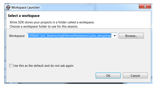
- In the SDK Work Space Launcher choose the path as “C:\Zynq7000AP_SoC_RedirectingEthernetPacketstoCache_design\sw” directory and select OK.
Setting up the workspace - After the SDK tool is launched, run the Target Communication Frame (TCF) agent on a Windows 64-bit machine. To do this, in SDK tool, Select Xilinx Tools > Launch Hardware Server.
- Select Xilinx Tools > Configure JTAG Setting
- The Configure JTAG Settings wizard opens.
- In the wizard, under the JTAG Cable > Type drop-down menu, select Xilinx TCF cable and Click OK.
- In SDK create a new application project. Select File > New > Application Project.
- The New Project wizard opens
- Use the information in the table below to make your selections in the wizard screens.
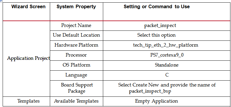
- Click Finish.
- The New Project Wizard closes and SDK creates the packet_inspect project and the packet_inspect_bsp BSP project under the project explorer. SDK also automatically compiles the project and generates the BSP.
- In the Project Explorer tab, expand the packet_inspect project, right-click the src directory, and select Import to open the Import dialog box.
- Expand General in the Import dialog box and select File System.
- Click Next.
- Add the files present in “C:\Zynq7000AP_SoC_RedirectingEthernetPacketstoCache_design\sw\srcs\” directory and click Finish.
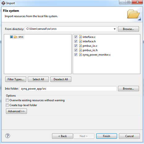
Importing the sources to the empty project - SDK automatically builds the application and displays the status in the console window.
- Expand the packet_inspect àsrc and open the xemacps_example_intr_dma.c.
- Observe the plain_test function at line number 1168.
- Observe the ppu_test function at line number 1290.
- After reviewing the code, close the file.
- Select Xilinx Tools à Program FPGA.
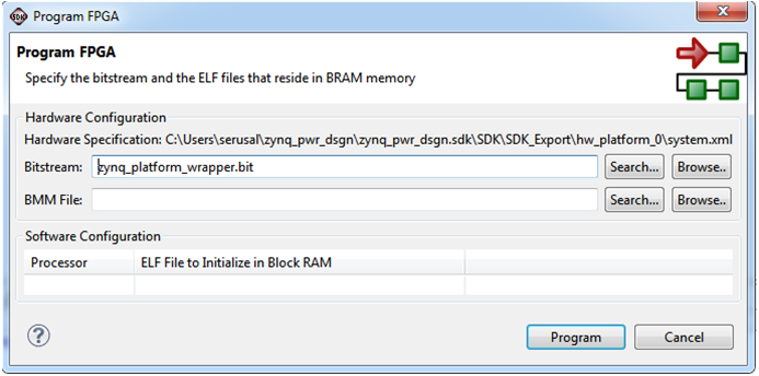
Programming the Zynq PL with bitstream - Delete any path specified in the BMM File Option.
- Click on Program to download the bitstream to the ZC706 board.
- Open a Serial Terminal (Like Hyperterminal or Teraterm) configured at following settings.
- Baudrate: 115200
- No of bits: 8
- Parity : 1
- Flow Control : NONE
- In the Project explorer view of the SDK tool, Right click “packet_inspect ” folder and select Run As à Run Configurations. This will launch the Run Configurations dialog.
- In the run configurations dialog , double click on Xilinx C/C++ ELF option to create a new configuration as shown below.
Creating A new Run Configuration - Select the packet_inspect_Debug configuration and click on Run.
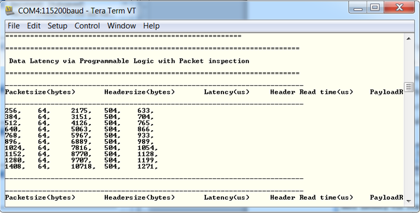
- Observe the message in the Serial console to view the results.
%20function%20Test%20Results..png?version=1&modificationDate=1536678091427&cacheVersion=1&api=v2)
plain_test() function Test Results - The first section of the test program runs the plain_test() function which runs the test as indicated in the Test Program Details Section in this Tech tip.
- The test program displays the number of Ethernet packets transmitted, the length of the Ethernet packets and the complete latency induced by the central interconnect for all the packets to get successfully transmitted and received at the Rx buffers in the DDR3 memory. The test Program also finally calculates the amount of time needed to successfully read 64 bytes of Ethernet Headers available in the DDR3 memory.
ppu_test() function Test Results. - The Second section of the test program runs the ppu_test() function which runs the test as indicated in the Test Program Details Section in this Tech tip. The test program displays the number of Ethernet packets transmitted, the length of the Ethernet packets and the complete latency of Ethernet packets which traversed through PS Ethernet and the PPU logic in the PL. The test Program finally calculates the amount of time needed to successfully read 64 bytes of all the Ethernet Headers available in the ACP memory compared to the 64 bytes of payload data available in the DDR3 memory.
6. Test Results:
6.1 Calculating Latency and Time Results for Ethernet Packet Traversing through the Central Interconnect.
The plain_test() function transmits 256 Ethernet Packets and calculates the latency from the time the Ethernet Transmit DMA starts transmitting all the packets until the Ethernet packets are received in destination memory locations specified in Receive Buffer Descriptor. |
| latcy calculated by plain_test() function |
Then the plain_test () function calculates the amount of time needed to successfully read 64 bytes of all the Ethernet Headers available in the DDR3 memory. The Ethernet packet is redirected to the DDR3 memory and the processor has to flush the cache to see the data available in the DDR3 memory. The following table provides you the test report of the time taken to route the Ethernet packets via the Ethernet Transmit and receive path via the central inter connect and the time taken to read the headers from the DDr3 memory.
| Packet Length |
Header Length |
Latency |
Header Read time in us |
| 256 |
64 |
1889 |
826 |
| 384 |
64 |
2680 |
963 |
| 512 |
64 |
3483 |
1144 |
| 640 |
64 |
4283 |
1281 |
| 768 |
64 |
5065 |
1442 |
| 896 |
64 |
5886 |
1597 |
| 1024 |
64 |
6672 |
1756 |
| 1152 |
64 |
7455 |
1922 |
| 1280 |
64 |
8285 |
2090 |
| 1408 |
64 |
9048 |
2258 |
6.2 Calculating the Latency and Time Results for Ethernet Packet Traversing through Programmable Logic
The ppu_test() function transmits 256 Ethernet Packets and calculates the latency from the time the Ethernet Transmit DMA starts transmitting all the packets until the Ethernet packets are received in destination memory locations specified in Receive Buffer Descriptor.Then the ppu_test () function calculates the amount of time needed to successfully read 64 bytes of all the Ethernet Headers available in the Cache. In this case the DDR3 memory does not need to flush the cache as the Ethernet Header data is already present in the memory. So the time that it takes to read the Ethernet headers is nothing but the time to read the data from the cache instead of flushing and invalidating the cache.
|
| Latency calculated by the ppu_test() function |
The following table provides you the test report of the time taken to route the Ethernet packets via the Ethernet Transmit and receive path and via the Programmable Logic and the time taken to read the headers from the Cache and the payload information of the same size from the DDR3 memory.
| Packet Length (bytes) |
Header Length(bytes) |
Latency (us) |
Header Read time (us) |
Data Read Time (us) |
| 256 |
64 |
2160 |
482 |
814 |
| 384 |
64 |
3099 |
482 |
942 |
| 512 |
64 |
4050 |
482 |
1112 |
| 640 |
64 |
4984 |
482 |
1240 |
| 768 |
64 |
5952 |
482 |
1389 |
| 896 |
64 |
7018 |
482 |
1542 |
| 1024 |
64 |
8128 |
482 |
1688 |
| 1152 |
64 |
9098 |
482 |
1844 |
| 1280 |
64 |
9891 |
482 |
1998 |
| 1408 |
64 |
10639 |
482 |
2155 |
6.3 Analyzing Packet latency.
As per the above data we have plotted the graphs of the latency of the Ethernet Packet Traversing through Programmable Logic vs. the latency of the Ethernet Packet Traversing through Central Interconnect.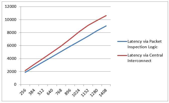 |
| Graph 1: Latency (Y-axis/Units: us) vs. Packet Size (X-axis /Units: bytes) |
In this graph we have seen that the latency of the programmable logic is more as it contains the delay induced by the central Interconnect and buffer time needed for the packet inspection logic present in the PL.
6.4 Analyzing Packet Header Read Time.
At the same time if we look at the processor overhead performance we have also calculated the time taken to read the headers while the Ethernet Packet is redirected to DDR3 via central Interconnect and calculated the time taken to read the headers while the Ethernet Packet is redirected to PL logic and routed via ACP port to L2 cache memory.As per the above data we have plotted the graphs of the performance improvement has been analyzed.
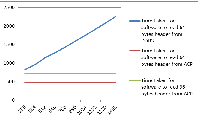 |
| Graph 2: Header Read time (Y-axis/Units: us) vs. Packet Size (X-axis /Units: bytes) |
In this graph we have seen that the software takes much more time to process Ethernet header if the packet is routed to DDR3 directly as this frequently needs flushing of the cache to have the updated data in the processor memory.
In the case of redirecting the Ethernet Header to the L2 cache via the Zynq ACP port, the Ethernet header is directly available in the Processors memory and no cache flushing is required and the time taken to read from the cache remains constant for a given number of Ethernet headers available in the memory.
8. Appendix A: File Descriptions in the Zynq7000AP_SoC_Ethernet_Packet_Redirection_Design.zip directory
- Zynq7000AP_SoC_Ethernet_Packet_Redirection_Design/tech_tip_eth_1:
- o XPS Design Project directory: Contains the supported design files for the tech tip.
- Zynq7000AP_SoC_Ethernet_Packet_Redirection_Design\sw\srcs
- o Contains Source files for the SDK project.
- § testperiph.c: Top level application software running the test programs for Interrupt and PS Ethernet
- § xemacps_example_intr_dma.c: Application program for testing single Ethernet loop back program.
- § Contains other supporting application files required for testing Ethernet hardware.
- o Contains Source files for the SDK project.
9. Appendix B : Description of the Ethernet Packet Processing unit
9.1 Ethernet Packet Processor
The Ethernet Packet Processor IP is a custom IP which has full memory mapped AXI4 (or AXI Lite) interface for both Master and Slave ports. The Ethernet Packet Processor IP performs the packet stripping as per what the software driver requests to do. |
| Inside the Ethernet Packet Processor |
9.1.1 Port Description:
- 1- Control Port: AXI4 Slave interface connected to the MAXI GP0 port.
- 1- Data Port : AXI4 Slave interface connected to the MAXI GP1 port.
- There are two AXI4 Master ports :
- AXI4 Master Header Port connected to the ACP interface
- AXI4 Master Payload port connected to the HP0 interface
The AXI 4 Master Header port is connected to the ACP interface via the Interconnect. The AXI4 Master Payload port is connected to the HP0 interface via the Interconnect. There are additional two output pins that can be used interrupt the ACP and the HP0 port.
- interrupt_in. Indicates the ETHERNET Controller has placed the packets in the memory.
- interrupt_out : Indicates the processor has done processing payload
9.2 Block Wise Description
9.2.1 Slave Side Registers
The Slave interface provides access to the following user logic software registers1) Control and Status Registers( CS1) ( 0x40000000 to 0x4000FFFF)
- Control Register (R/W)
- RX Buffer length Control Register (R/W)
- Status Registers (RO)
- Status_Flags_Header SM (RO)
- Status_Flags_Payload SM (RO)
- BD Counter (RO)
- Packet Counter (RO)
- Command State Machine Status
- Fifo Status Register 0 (RO)
- Fifo Status Register 1 (RO)
3) FIFO Data Register( CS2) ( 0x40020000 to 0x4002FFFF)
9.2.1.1 Control Register ( 0x40000000)
The following describes the nature of the Control Bits.| Bit Position |
Name |
Description |
| 0 |
ppu_go |
Starts the Packet Processing unit. This bit has to be set after every BD is processed. |
| 1 |
fifo_flush |
Flush the FIFO Unconditionally. This will also update the Packet drop counter.(TBD) |
| 2-6 |
Reserved |
|
| 7 |
sw_reset |
Soft reset the Packet Processing unit. (TBD) |
| 8-31 |
Reserved |
9.2.1.2 RX Buffer length Control Register ( 0x40000004)
Programs the number of RX Buffers to be used. The header manager and the Payload manager state machines will this is Number to write the frames in the memory in a round robin fashion.| Position |
Byte3 |
Byte2 |
Byte1 |
Byte 0 |
| Name |
No of RX Buffers |
|||
9.2.1.3 STATUS Register ( 0x40000008)
| Bit Position |
Name |
Description |
| 0 |
start_header_transmit |
Header Transmisson has started |
| 1 |
start_payload_transmit |
Payload Transmission has started. |
| 2-31 |
Reserved |
9.2.1.4 Status_Flags_Header SM ( 0x40000018)
| Position |
Byte3 |
Byte2 |
Byte1 |
Byte 0 |
| Name |
Reserved |
|||
9.2.1.5 Status_Flags_Payload SM ( 0x4000001c)
| Position |
Byte3 |
Byte2 |
Byte1 |
Byte 0 |
| Name |
Reserved |
|||
9.2.1.5 BD Count Register ( 0x40000010)
Displays the Number of BD’s Processed. Increments by one after all packets in BD are transmitted.| Position |
Byte3 |
Byte2 |
Byte1 |
Byte 0 |
| Name |
BD Count |
|||
9.2.1.6 Packet Count Register ( 0x40000014)
Displays the Number of Packets processed .| Position |
Byte3 |
Byte2 |
Byte1 |
Byte 0 |
| Name |
No of RX Buffers |
|||
9.2.1.7 FIFO STATUS Register0 ( 0x4000000c)
Displays the FIFO 0 status .| Bit Position |
Name |
Description |
| 0 |
Fifo _full |
Indicates FIFO is full |
| 1 |
wr_error |
Indicates the FIFO Over flow has occured |
| 2 |
wr_ack |
Write Successful |
| 4 |
rd_error |
READ Over Run |
| 5 |
data_valid_i |
READ VALID |
| 6 |
empty |
FIFO is Empty |
9.2.1.8 FIFO STATUS Register1 ( 0x4000000c)
Displays the FIFO 1 status .| Bit Position |
Name |
Description |
| 0 |
Fifo _full |
Indicates FIFO is full |
| 1 |
wr_error |
Indicates the FIFO Over flow has occured |
| 2 |
wr_ack |
Write Succeffull |
| 4 |
rd_error |
READ Over Run |
| 5 |
data_valid_i |
READ VALID |
| 6 |
empty |
FIFO is Empty |
9.2.1.9 RX Buffer Address: ( 0x40010000)(readonly)(512 memory locations ,32 bit)
The RX Buffer Address array stores the base addresses of the RX buffers that are defined by the Buffer descriptors provided in the memory. The addresses in this array are programmed when the Buffer descriptors are initialized for the Ethernet DMA driver.
The size of the RX Buffer Address array is 64 bit wide x 256 deep. The depth of the RX Buffer Address Memory can be resized for the number of Buffer descriptors through the RX Buffer Address Size register.
The top 32 bit stores the address of the RX Buffer Address and the lower 32 bit displays the status of the packet.
DWORD 0
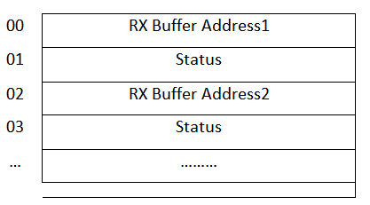
DWORD 1
| Bit Position |
Name |
Description |
| [11:0] |
Length of Packet |
Displays the Length of the packet received |
| 13 |
header_processing_done |
This bit indicates that the Header Manager State machine has successfully processed the header portion of the Ethernet Frame. |
| 14 |
payload_processing_done |
This bit indicates that the Payload Manager State machine has successfully processed the payload portion of the Ethernet Frame. |
| 15 |
bdring_processed |
This bit indicates that the BD has been processed. |
| [31:16] |
Packet type |
Displays the type of the packet received |
The RX Buffer Address array stores the base addresses of the RX buffers that are defined by the Buffer descriptors provided in the memory. The addresses in this array are programmed when the Buffer descriptors are initialized for the Ethernet DMA driver.
The size of the RX Buffer Address array is 64 bit wide x 256 deep. The depth of the RX Buffer Address Memory can be resized for the number of Buffer descriptors through the RX Buffer Address Size register.
The top 32 bit stores the address of the RX Buffer Address and the lower 32 bit dipsys the status of the packet.
9.2.1.10 Dual FIFO
There is a 400 dword deep dual FIFO (each capable of holding 1600 bytes) is provided in the Ethernet Packet Processor logic capable of the handling one BD of data, which is the maximum data that the Ethernet DMA can push over the AHB bus to the central interconnect.
9.2.1.11 Header Manager
The Function of the Header Manager is to assemble the burst packets for the Master Header Port.
The Header Manager copies the address from RX Buffer Address Memory and writes the address to the slave connected on the Master Header Port via the Master Write Address port.
Then the Header Manager performs AXI4 Data Writes to the slave connected on the Master Header Port via the Master Write Data port.
The length of the Data Burst is defined by the Header length register.
9.2.1.12 Payload Manager
The Function of the Payload Manager is to assemble the burst packets for the Master Payload Port.
The Payload Manager copies the address from RX Buffer Address Memory adds the header length to it (this is the effective address to where the payload needs to be written in the RX Buffer) and writes the address to the slave connected on the Master Payload Port via the Master Write Address port.
Then the Payload Manager performs AXI4 Data Writes to the slave connected on the Master Payload Port via the Master Write Data port.
The length of the Data Burst will be Frame length – Header Length.
-----------End of Tech Tip-------------------
© Copyright 2019 - 2022 Xilinx Inc. Privacy Policy