KCU105 SGMII over LVDS design creation using board flow
KCU105 SGMII over LVDS design creation using board flow
This is the an example of how to use board flow to create SGMII over LVDS design on KCU105 in Vivado 2017.2; and use LWIP echo application in SDK to verify the link.The project is attached here:
Below are the detailed steps:
1) Create a project for KCU105 board part and create a new block design.
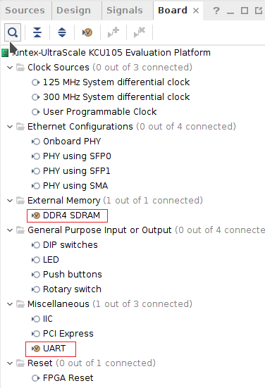
2) From board Tab, drag and drop DDR4_SDRAM and UART interfaces into IPI Canvas.
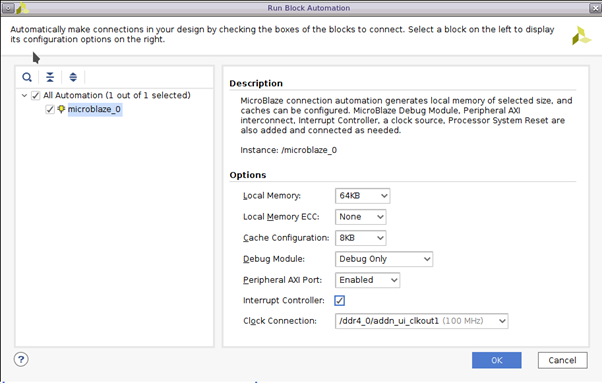
3) Add microblaze and Run Block Automation for 64 KB of local memory and enable interrupt controller for that.
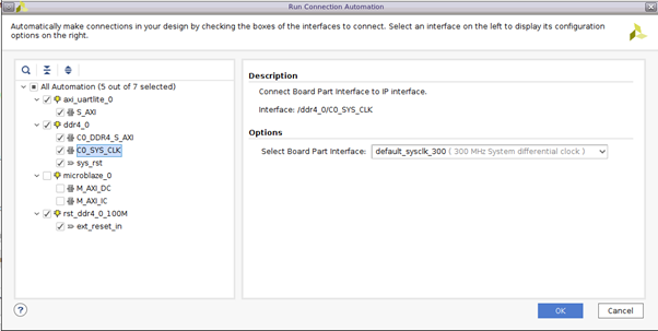
4) Run Connection Automation and select all to connect AXI interfaces of MIG, UARTLITE IPs and their clocks and resets.
- Uncheck the microblaze_0 part of it
- Make sure C0_SYS_CLK interface for MIG shows default_sysclk_300 selected
- C0_DDR4_S_AXI is connected to /microblaze_0 (Cached) and clock connection of Auto
- All other AXI interfaces and Microblaze clock are connected to 100 MHz additional clock output of MIG
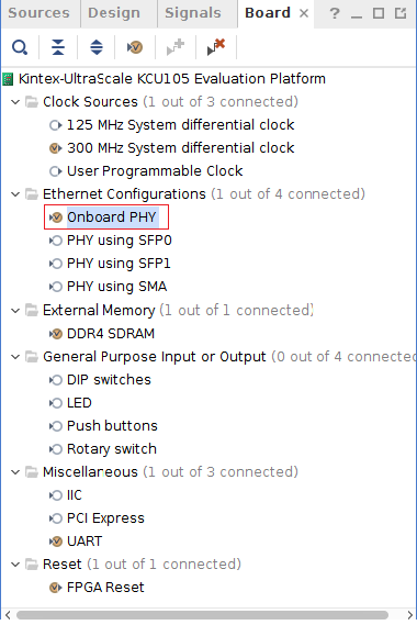
5) Drag & Drop On board PHY interface into IPI Canvas. This will add AXI Ethernet IP and connect SGMII interface.
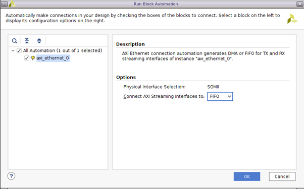
6) Run Block Automation for AXI Ethernet and select "FIFO" for AXI Streaming interface.
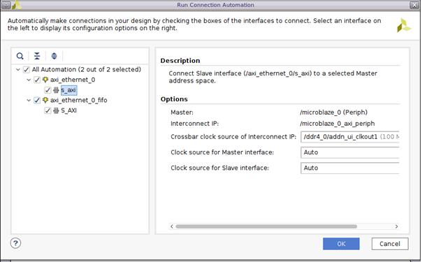
7) Run Connection automation.
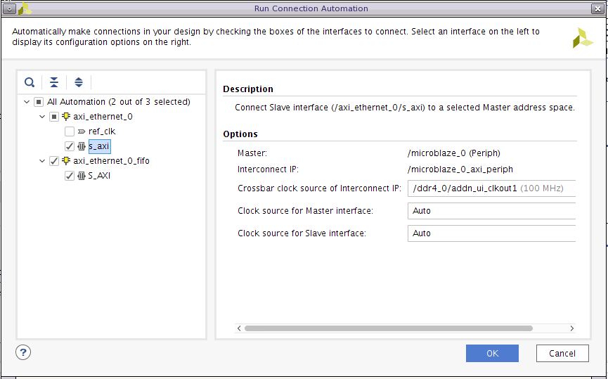
- In AXI Ethernet, for s_axi, clock connection is made from 100MHz MIG additional clock.
- Similarly for s_axi interface in axi_ethernet_0_fifo, select clock connection as 100 MHz MIG additional clock.
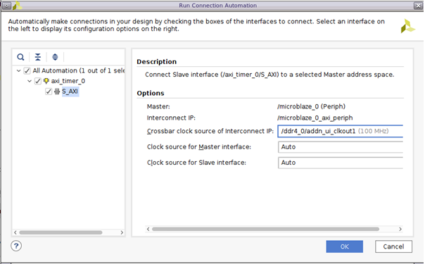
8) Add AXI Timer into IPI Canvas.
- Make sure the s_axi_aclk is connected to 100 MHz MIG additional clock.
9) Change Concat to have 3 input ports. Connect one input of Concat to Interrupt output of AXI_Ethernet and other input to Interrupt output of axi_ethernet_0_fifo, and one connected to the interrupt output of AXI Timer
10) Save the BD and generate wrapper.
11) Implement the design and generate bitstream.
12) Export Hardware and bitstream in SDK.
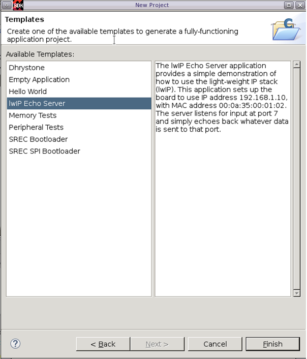
13) Launch SDK and Create Xilinx Application Project – LWIP Echo Sever; and built the application.
14) Start XMD console.
15) Run following commands:
- fpga –f design_1_wrapper.bit
- connect mb mdm
- dow lwip.elf
- con

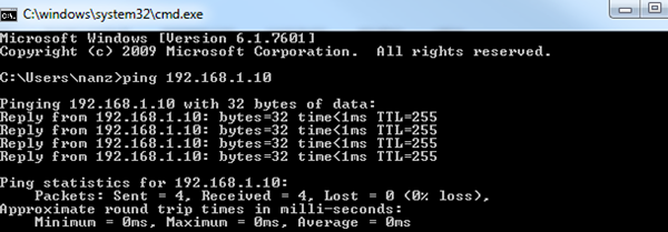
17) In cmd, you should be able to ping:
Changing the design to test SFP slots.
Alternatively, users can test PHY using SFP0/SFP1 or SMA. To change to this, in board flow, from step 5) above:
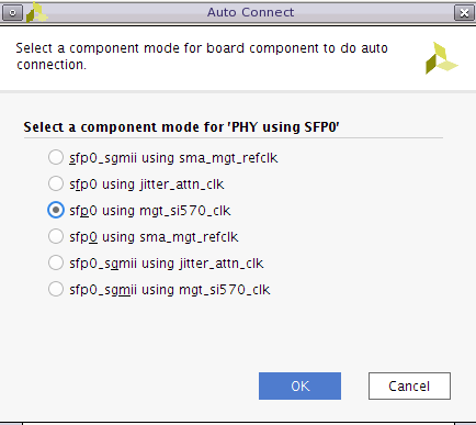
5) Drag & Drop “PHY using SFP0” into IPI Canvas. This will add AXI Ethernet IP. And choose sfp0 using mgt_si570_clk.
6) Run Block Automation for AXI Ethernet and select "FIFO" for FIFO_DMA interface.
7) Run Connection Automation.
- Deselect ref_clk from axi_ethernet_0.
- Make sure the clock of s_axi and s_axi interfaces of axi_ethernet_0 and axi_ethernet_0_fifo is using DDR additional clock 100MHz.
8) Generate a 50MHz from DDR4; and connect it to the ref_clk from axi_ethernet_0.

9) Connect the interrupt ports of axi_ethernet_0 and axi_ethernet_fifo to the Concat.
10) Add AXI Timer into IPI Canvas and make sure the s_axi_aclk is connected to 100 MHz MIG additional clock.
11) Change Concat to have 3 input ports; and connect the interrupt port of AXI Timer to the 3rd input of Concat.
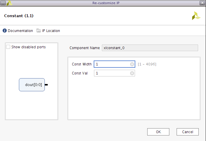
12) Add a Constant module and connect the output to signal_detect from AXI Ethernet core.
13) Continue the step 10) to step 13) above.
14) Before powering on KCU105, open the com port with 115200 baud rate.
15) Power on KCU105.
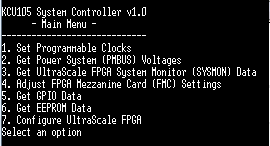
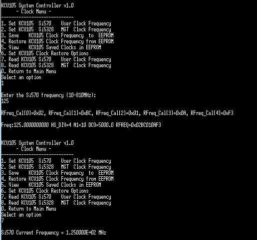
16) Set the si570 clock to 125MHz
17) Continue from step 14) to step 15) above.
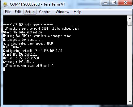
18) You should see the following in hyper terminal.
19) You should be able to ping the board through SFP0.
PS: the same method can be used to test other SFP0 or SMA ports.
© Copyright 2019 - 2022 Xilinx Inc. Privacy Policy